GPS Spoofing Detection System
Ongoing ProjectProject Overview
Department: Electronic & Telecommunication Engineering, University of Moratuwa
Role: RF & Hardware Engineer
GNSS spoofing on the GPS L1 band (1575.42 MHz) poses a critical threat to navigation systems, autonomous vehicles, and timing infrastructure worldwide. Our final-year project addresses this security challenge by developing a complete spoofing detection system that integrates custom RF hardware with machine learning algorithms.
The system combines three key components: a custom-designed RHCP patch antenna optimized for GPS L1, a high-performance RF front-end for signal acquisition and conditioning, and a machine-learning pipeline for intelligent spoofing detection. My contribution focuses entirely on the RF hardware domain, encompassing antenna design, electromagnetic simulation, and front-end PCB development.
My Contributions
1. RHCP Patch Antenna Design (GPS L1 – 1575.42 MHz)
I designed and optimized a Right-Hand Circularly Polarized microstrip patch antenna specifically for GPS L1 reception. This antenna serves as the critical first element in the signal chain, capturing satellite signals with optimal polarization matching and minimal interference.
Key Design Aspects:
- Substrate Selection: Precise material characterization considering dielectric constant (εᵣ), thickness, and loss tangent for optimal performance
- Patch Geometry: Calculated and refined patch dimensions for resonance at 1575.42 MHz with tight frequency tolerance
- Circular Polarization: Achieved RHCP through carefully designed perturbation techniques (corner truncation/dual-feed)
- Impedance Matching: Designed 50 Ω matching network using quarter-wave transformers and inset feed optimization
- Axial Ratio Optimization: Achieved axial ratio < 3 dB across the L1 band for high-quality circular polarization
- Radiation Pattern: Tuned far-field pattern for maximum gain in the zenith direction, ideal for overhead satellite reception
Simulation & Optimization:
Performed comprehensive electromagnetic analysis using Ansys HFSS, including parametric sweeps, optimization routines, and near-field/far-field pattern analysis.
Antenna Performance Achieved:
- Return Loss (S₁₁): < -20 dB at 1575.42 MHz
- Axial Ratio: < 3 dB across GPS L1 bandwidth
- Radiation Pattern: Stable RHCP with minimal cross-polarization
- Gain: Optimized for satellite link budget requirements
- Efficiency: Maximized through substrate and conductor loss minimization
2. GPS L1 RF Front-End PCB Design (Joint Contribution with Pramidu)
I collaborated with my teammate Pramidu to develop the complete GPS L1 front-end PCB, with clearly defined responsibilities. My role focused entirely on the RF aspects of the board including antenna integration, LNA circuitry, RF filtering, and impedance-controlled routing, while also serving as the lead engineer for overall PCB verification. This subsystem amplifies, filters, and conditions the weak satellite signals for reliable detection and analysis.
My Design Responsibilities (RF & Verification):
- LNA Selection & Design: Selected low-noise amplifier with optimal noise figure, gain, and linearity; performed DC biasing network design and stability analysis
- RF Circuit Simulation: Used Ansys SIwave for S-parameter analysis, transmission line modeling, and RF performance verification
- Bandpass Filter Design: Designed narrow bandpass filter centered at L1 frequency for out-of-band interference rejection
- Impedance Matching Networks: Implemented distributed/lumped element matching for 50 Ω system impedance throughout the RF signal chain
- RF PCB Layout: Executed controlled impedance microstrip/stripline routing with precise trace width calculations and length constraints
- RF Grounding Strategy: Implemented solid ground plane, via stitching, and compartmentalized grounding for RF sections and EMI/EMC compliance
- Antenna Integration: Designed RF interface between RHCP patch antenna and front-end circuitry with proper impedance matching
- Overall PCB Verification: Led complete design verification including DRC, signal integrity analysis, and pre-fabrication validation
- Gerber Review & Sign-off: Performed final verification of fabrication-ready files before submission to PCB manufacturer
Collaborative Design Elements:
Pramidu contributed to the digital interface sections, power distribution network, and supporting circuitry, while I maintained responsibility for all RF-critical design elements and performed comprehensive design verification across the entire board to ensure integration and manufacturability.
Tools & Workflow:
- Ansys SIwave: RF circuit simulation, S-parameter extraction, signal integrity analysis, and impedance verification
- Altium Designer: Complete schematic capture, multi-layer PCB layout, and design rule checking (DRC)
Note: This PCB was developed in collaboration with my teammate Pramidu. I focused on RF design and led overall verification, while Pramidu contributed to digital interfaces and power distribution.
3. PCB Design & Signal Integrity Analysis (RF Lead & Overall Verification)
The GPS L1 RF front-end PCB was designed collaboratively with Pramidu, with my primary focus on high-frequency signal integrity, RF impedance control, and electromagnetic compatibility of the RF sections. As the RF lead and overall verification engineer, I was responsible for ensuring the complete design integrates the RHCP antenna, LNA, filtering, and signal conditioning circuitry on a multi-layer board optimized for 1575.42 MHz operation.
3D PCB Visualization in Altium Designer
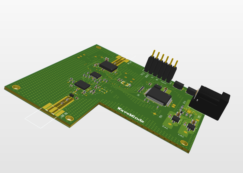
3D PCB Rendering: Complete GPS L1 RF front-end PCB showing component placement, RF trace routing, and antenna integration area. The 3D model validates mechanical clearances and visualizes the complete hardware assembly.
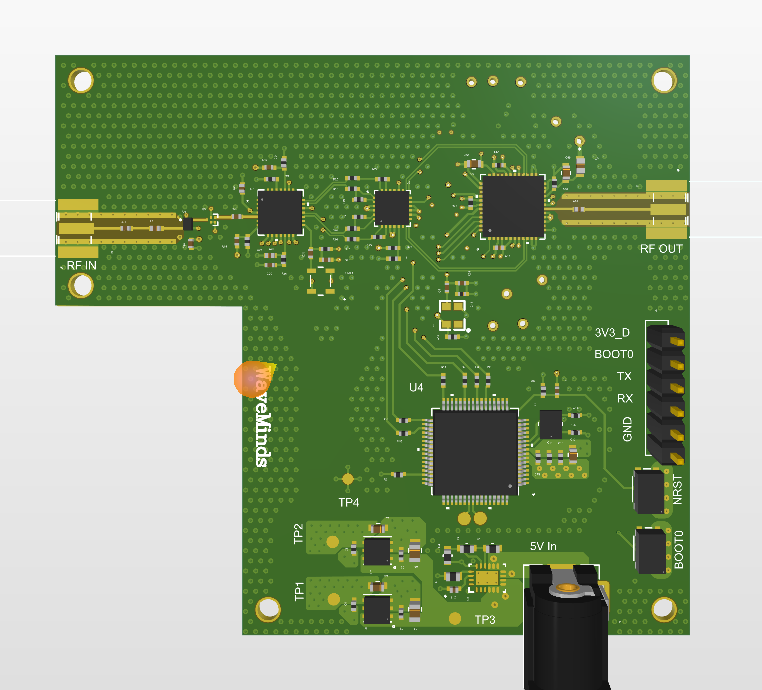
Top Layer View: RF component placement and signal routing strategy. Notice the compartmentalized layout separating RF sections, controlled impedance traces, and strategic via placement for optimal grounding.
Signal Integrity & Impedance Analysis (Ansys SIwave)
As the verification lead, I performed comprehensive signal integrity and impedance analysis using Ansys SIwave to ensure reliable RF performance at 1575.42 MHz. This involved extracting the complete PCB stackup, analyzing transmission line characteristics, and verifying 50 Ω impedance throughout the RF signal chain with rigorous pre-fabrication validation.
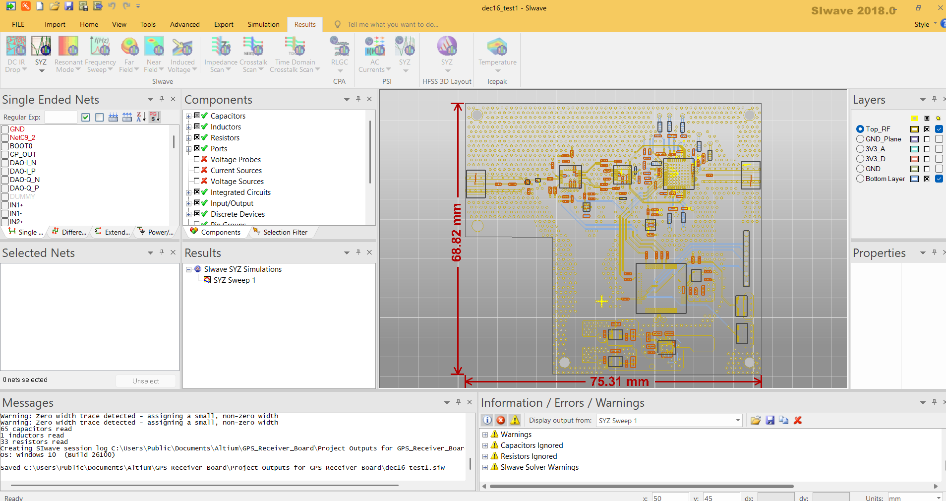
PCB in Ansys SIwave: Imported PCB design from Altium for full-wave electromagnetic analysis. SIwave enables extraction of S-parameters, impedance verification, and transmission line characterization for critical RF traces.
Transmission Line Impedance Matching to 50 Ω
Maintaining consistent 50 Ω characteristic impedance across all RF traces is critical for minimizing reflections and ensuring maximum power transfer. I designed microstrip transmission lines with precise trace widths calculated based on the PCB stackup (substrate height, dielectric constant, and copper thickness).
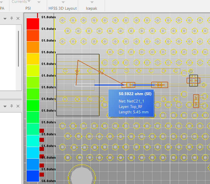
50 Ω Impedance Matching: Analysis of transmission line impedance across frequency. The plot confirms that the RF traces maintain 50 Ω ± tolerance across the GPS L1 band (1575.42 MHz), ensuring minimal signal reflections and optimal power transfer.
S-Parameter Analysis: S₁₁ and S₂₁ of RF Traces
S-parameter measurements quantify the RF performance of transmission lines. S₁₁ (return loss) indicates how well the trace is matched to 50 Ω—lower S₁₁ values mean less reflected power. S₂₁ (insertion loss) shows signal transmission efficiency through the trace—higher S₂₁ values indicate minimal loss.
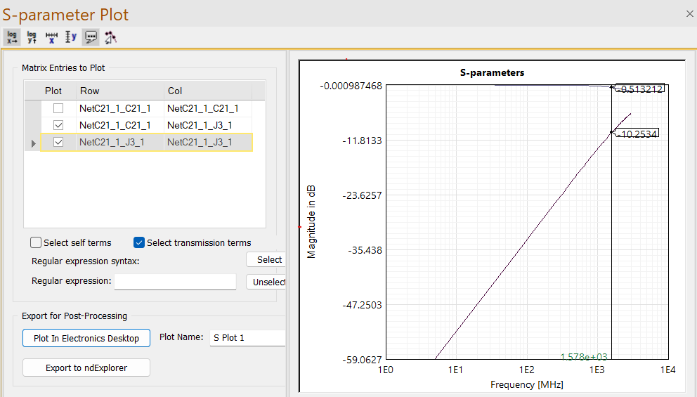
S-Parameter Analysis (Input RF Trace): Simulated S₁₁ (return loss) and S₂₁ (insertion loss) for the input transmission line feeding the LNA. The results show good impedance matching with S₁₁ ≈ -10 dB at 1575.42 MHz, indicating acceptable reflections for the GPS L1 application, and S₂₁ ≈ -0.5 dB showing minimal insertion loss—critical for preserving the weak GPS signal strength.
Key SI/PI Analysis Results:
- Return Loss (S₁₁): ≈ -10 dB at GPS L1 frequency → good impedance matching suitable for GPS applications
- Insertion Loss (S₂₁): ≈ -0.5 dB → minimal trace loss, preserving signal integrity
- Characteristic Impedance: 50 Ω ± 5% tolerance maintained across all RF traces
- Via Transitions: Optimized via diameter and anti-pad clearance for minimal discontinuities
- Crosstalk Analysis: Adequate trace separation ensuring minimal coupling between RF paths
- Ground Plane Continuity: Verified solid ground return paths with via stitching every λ/20
4. Current Project Status (January 2026)
- ✅ RHCP patch antenna design completed and prototype fabricated
- ✅ Full RF front-end PCB design finalized in Altium Designer
- ✅ Signal integrity and impedance analysis completed using Ansys SIwave
- ✅ S-parameter verification: S₁₁ ≈ -10 dB, S₂₁ ≈ -0.5 dB at GPS L1 frequency
- ✅ Gerber files submitted for professional PCB fabrication
- 🔄 Project currently in PCB manufacturing stage
- ⏳ Upcoming: Hardware testing, VNA measurements, and system calibration
- ⏳ Planned: Integration with DSP/ML pipeline and end-to-end system validation
Technical Skills Demonstrated
Antenna Design
RHCP microstrip patch antenna design and optimization for GNSS applications
EM Simulation
High-frequency electromagnetic analysis using Ansys HFSS with parametric optimization
RF Circuit Design
LNA, BPF, and matching network design with ADS simulation and analysis
RF PCB Layout
Controlled impedance routing, grounding strategies, and EMI mitigation techniques
Signal Integrity
S-parameter analysis, impedance verification, and transmission line optimization using SIwave
System Integration
RF front-end integration with DSP/ML pipelines for complete system functionality
GNSS Technology
GPS L1 band operation, satellite signal characteristics, and navigation security
3D PCB Modeling
3D visualization and mechanical validation using Altium Designer's 3D engine
Tools & Technologies
Project Significance
This final-year project strengthens my core expertise in multiple critical areas of RF engineering:
- RF & Microwave Engineering: Hands-on experience with real-world RF system design from concept to fabrication
- GNSS/L-Band Development: Deep understanding of satellite navigation systems and L-band antenna engineering
- RF Front-End Systems: Complete signal chain design including LNA, filtering, and signal conditioning
- Secure Navigation Hardware: Addressing critical cybersecurity challenges in navigation infrastructure
Career Positioning
This project positions me strongly for future opportunities in:
- RF/Microwave Design: Communication systems, radar, and wireless infrastructure
- GNSS Receiver Development: Navigation systems for automotive, aerospace, and consumer electronics
- Aerospace Electronics: Satellite communication, avionics, and space-grade hardware
- Defence Systems: Secure communication, electronic warfare, and navigation security
- Communication Hardware R&D: Next-generation wireless systems and IoT connectivity
Key Learnings
- Comprehensive understanding of RHCP antenna design principles and circular polarization techniques
- Advanced electromagnetic simulation methodology and optimization workflows in HFSS
- RF circuit design fundamentals: LNA stability, noise analysis, and gain-bandwidth optimization
- High-frequency PCB design best practices: controlled impedance, via stitching, and EMI suppression
- Signal integrity analysis using Ansys SIwave: S-parameter extraction, impedance verification, and transmission line characterization
- S₁₁ and S₂₁ measurement interpretation for RF trace performance validation
- 3D PCB visualization and mechanical design validation using Altium Designer
- System-level thinking: integrating RF hardware with digital signal processing and ML algorithms
- Project management in multidisciplinary team environment with hardware/software integration
- GNSS signal characteristics, satellite link budgets, and navigation system vulnerabilities